Dr. Bob’s Nickel’s Worth: Nickel Underplates
By Dr. Robert S. Mroczkowski, Bishop & Associates
October 2012
One of the things Max commented on in his recent article was the departure of “gray beards” — the “old guard” of connector technology/wisdom, of which he is a prime example. Max noted that the basic papers on nickel underplate development/research are generally no longer available. While that is true, I would like to point out that there are at least two sources that reference and discuss some of those papers. I humbly mention my Electronic Connector Handbook (which is out of print but available from Knovel), in particular Chapter 3, and Electrical Contacts: Principles and Applications, edited by Paul Slade. Chapters 6 and 7 were written by Mort Antler, one of the major researchers of the importance of nickel underplates in electronic connectors.
The generally specified range of nickel thickness for an underplate for gold is 50 to 100 microinches (1.25 to 2.5 microns). The lower limit is necessary to provide enough nickel thickness to reduce the overall porosity of the gold-over-nickel finish and provide an adequate diffusion barrier as well as sufficient composite hardness of the gold-over-nickel system to enhance the mating durability of the connector. The upper limit is influenced by the tendency towards increasing surface roughness and decreasing nickel ductility as the plating thickness increases. As Max noted, the plating process, including plating bath selection, is critical to both the increase in roughness and the decrease in ductility. The 150 microinches cited may be considered in higher temperature applications where diffusion related degradation may increase in importance.
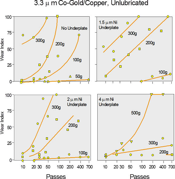
The relationship between contact wear and nickel thickness can be seen by consideration of Figure 1, taken from Antler, which shows the plating wear index (WI), which is the wear-through of the gold to the underlying metal, versus the number of passes (“mating” events) for varying nickel plating thicknesses and contact forces. The gold thickness of 3.3 microns (130 microinches) is higher than current gold thickness values, but back in the 1970s, telecom applications (Antler was at Bell Laboratories Murray Hill, NJ) approached those values (with gold at $35/oz).
The WI indicates the percentage of the sliding track that shows exposed copper. The copper base metal, lower in hardness than the copper alloys typically used in connectors, and the un-lubricated surface make this combination a higher wear system than typical of connectors today. The essence of the data can be realized by following the 200-gram contact force data (higher than typical electronic connectors today) for each of the nickel thicknesses (0, 60, 80, and 160 microinches). 100 WI occurs for 0 nickel at 100 passes; at 600 passes for 1.5 microns Ni; the 2.0 micron data extrapolates to about 1,500 passes; and the 4 micron data shows a WI of about 10% after 700 cycles. Wear resistance increases dramatically with nickel thickness over this thickness range.
Generally speaking, hard materials have better wear resistance than soft materials. As the nickel thickness increases, the composite hardness of the contact finish and base metal increases and the wear rate decreases. This is arguably one of the more important functions of the nickel underplate, because it improves the mating durability and, therefore, the number of mating cycles a connector can support before the contact finish is lost. Remember, however, the downside of increasing nickel roughness could significantly compromise this benefit at higher nickel thicknesses.
One more nickel issue merits attention: the oxide layer that is essentially intrinsic to nickel. Nickel will oxidize very rapidly, but to a limited thickness, on the order of 10 nanometers (0.01 microns). This oxide layer is very hard and is a p-type semiconductor. The combination of hard oxide over hard base metal increases the difficulty of mechanical displacement of the oxide. The contact resistance to a nickel surface will be increased by the oxide layer, unless that layer is disrupted electrically, meaning dielectric breakdown. The breakdown voltage of nickel is of the order of a volt, which is why it is useful as a battery contact material. But the nickel oxide is not an issue in gold/nickel-plated contact systems, because the oxide has been removed, by necessity, during the plating process. Gold will not plate onto an oxide coated nickel surface, which is a key issue, known as passivated nickel, to platers. There will be a nominal increase in contact resistance due to the higher resistivity of nickel compared to copper alloys and gold (nickel has about 10 times the resistivity of copper) but the increase will be small given the low thickness of the nickel layer.
For completeness, I should note that, due to the nickel oxide, nickel is susceptible to fretting corrosion. And, on that note, I can hear Max saying, “Remember that when you specify a gold flash over nickel contact plating.”
- Nanocrystalline Silver Alloy Contact Finishes in Electronic Applications - April 6, 2015
- Nanocrystalline Silver Contact Platings - March 16, 2015
- Dr. Bob on Gold Flash Contact Finishes (and Max Peel) - September 22, 2014