Moore’s Law: Technology Evolves to Meet Its End
The end of Moore’s Law will occur in the 2020s, but we can already see evidence of and fallout from the imminent event.
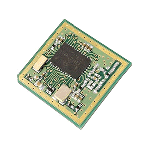
Photo courtesy of Silicon L
The $400B semiconductor market is approaching the end of Moore’s Law as we have known it. This will occur around the middle of the 2020s because feature sizes will become too small for existing process technology as traces approach molecular size.
But long before that – now – we can see that changes will be evolutionary. Companies are finding that 3D silicon structures can solve many application challenges that the planar IC circuit, which has been employed since the IC’s inception, can’t. The reason for this shift is both technologic and economic. New silicon fabs cost billions, so companies need to band together to cover these costs or find another way. In addition, IC fabrication has developed to the point where silicon microvia technology is now a production tool with the ability to stack ICs to gain additional functionality in same/similar spaces. Additionally, advances in IC packaging – specifically the so-called System in Package (SiP) – has become widely available with organic substrates.
The Apple iPhone and iWatch employ SiPs due to space constraints and economics. Photonics applications such as the PSMC silicon photonics initiative, spearheaded by MIT and iNEMI, will roadmap emerging silicon photonics (SiPh) technology through the 2020s. Industry will use vertical-cavity indium phosphide (InP) lasers, detectors, and silicon driver chips in a small SiP package. As time progresses, optical silicon will be perfected and optical waveguides will be used in the SiP or System-on-Chip (SoC) package substrate to optically connect with a perimeter or vertical interposer or socket. Optical connections in the PCB will be waveguides or fiber, connecting to surface-layer SMT fiber optic connectors.
The whole system will have to be single-mode as in-package/in-system data rates reach 100Gb/s to 1000Gb/s.
During a conference at Massachussetts Institute of Technology in April, many solutions were proposed by tier-one equipment and chip manufacturers, but one got the impression that a lot of exciting work is being done at the chip, package, and interconnect levels. It sounds like we are not too far from initial production of several of these solutions.
So what we see here is not the end of Moore’s Law, per se, but the opportunity to find new silicon and silicon photonics solutions for future ultra-high-speed applications that will eventually reach the petabyte range. These solutions are necessary because copper can’t get us there and silicon photonics will. In addition, copper-silicon/CMOS circuitry will morph into 3D and SiP solutions, which in some cases will go full-bore into Systems-on-Chip. SoC is used now in compatible applications. The computer-on-chip with its micro-system bus, memory, chip-sets, and I/O is off in the distant future.
What does this mean for connector technology?
- Advanced fiber optic technologies and newer technologies for in-system interconnects
- Increased integration of circuitry closest to the chip
- Continued downward pressure on connector feature sizes
- Eventual collapse of the levels of packaging, with I/O becoming more dominant
- Fewer but more costly connectors per system
- More opportunities for value-added circuitry built into connector shells
- Many parallel solutions coming from smaller companies and startups
- More QSFP, QSFP24, and beyond
- Changes in high-speed backplane applications, including fiber optic cable
- Fiber optic versions of USB and LightPeak technologies and an optical RJ45
- Eventually a significant shift toward photonics technology in computer, server, data center, and other applications
- Copper will remain king in general circuitry applications with alloys approaching 100% conductivity
- Electric Vehicles Move into the Mainstream with New EV Battery Technologies - September 7, 2021
- The Dynamic Server Market Reflects Ongoing Innovation in Computing - June 1, 2021
- The Electronics Industry Starts to Ease Out of China - November 3, 2020
