Signal Integrity Measurement – Using Logic Analyzers
Signal Integrity Measurement – Using Logic Analyzers
Evolving technology makes it increasingly difficult for system developers to produce and maintain complete, unimpaired signals in digital systems. Tektronix has published a primer to provide some insight into signal integrity-related problems in digital systems, and to describe their causes, characteristics, effects, and solutions. To learn more about the utilization of logic analyzers, read the excerpt below. Visit Tektronix online to learn more about these products as well as other test technologies for signal integrity in the white paper, “The Fundamentals of Signal Integrity.”
Signal Integrity Measurement Requirements
Direct signal observations and measurements are the only ways to discover many causes of signal integrity-related problems. As always, using the right tool will simplify any task. Most signal integrity measurements are made with the familiar combination of instruments found in most electronics engineering labs: the logic analyzer, the oscilloscope, and, in some cases, the spectrum analyzer. Probes and application software to perform tasks like jitter analysis round out the basic toolkit. Signal sources can be used to provide distorted signals for stress testing and evaluation of new devices and systems. They can also provide missing system inputs or replicate sensor signals to the device during test. A time-domain reflectometry solution is helpful for tracking signal path impedance problems such as impedance mismatch and other signal integrity problems that cause reflections or amplitude loss.
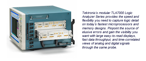
The logic analyzer is the first line of defense for digital troubleshooting, especially for complex systems with numerous buses, inputs, and outputs. A logic analyzer has the high channel count to acquire digital information from many test points and then display that information coherently to identify problems.
Because it’s a digital instrument, the logic analyzer detects threshold crossings on the signals it’s monitoring then displays the logic signals. The resulting digital waveforms are clear and understandable, and can easily be compared with expected data to confirm that the device is working.
These waveforms are usually the starting point in the search for problems that compromise signal integrity.
Logic analyzers offer two different data acquisition modes: “state” and “timing.” State (or synchronous) acquisition is used to acquire the “state” of the device under test (DUT). A signal from the DUT defines when and how often data will be acquired. The signal used to clock the acquisition may be the device’s clock, a control signal on the bus, or a signal that causes the DUT to change states. Data is sampled on the active edge and represents the condition of the DUT when the logic signals are stable.
Timing (or asynchronous) acquisition captures signal timing information to create timing diagrams. In this mode, a clock internal to the logic analyzer is used to sample data. There is no fixed timing relationship between the target device and the data acquired by the logic analyzer. This mode is used when a long, contiguous record of timing details is needed.
Triggering flexibility is the key to fast, efficient detection of unseen problems. In a logic analyzer, triggering is used to set conditions that, when met, will tell the logic analyzer to acquire data and display the result. When a logic analyzer triggers on an error, it is proof that the error has occurred, which enables fast detection. Most logic analyzers today include triggers to detect events that compromise signal integrity, like glitches and setup and hold time violations.
A unique strength of a logic analyzer is that these trigger conditions can be applied across hundreds of channels at once. With its ability to analyze hundreds to thousands of digital lines at a time, the logic analyzer is a powerful tool for discovering device faults for further analysis. For fast and efficient debugging, it’s important to carefully look at usability features like triggering, as well as performance attributes, when choosing a logic analyzer solution.
A logic analyzer’s probing scheme plays a critical role in high-speed digital acquisition. It’s critical that the probe deliver the signal to the logic analyzer with the highest possible fidelity. Most logic analyzer probes fulfill this fundamental requirement, but some take the concept even further.
Some logic analyzers require separate probing connections for timing and state acquisitions. This is known as “double probing,” which is a technique that can compromise the signal environment, affecting the actual measurements themselves. For example, connecting two probes at once to the test point can create unacceptable levels of signal loading. Connecting them individually exposes the test point to double the risk of damage or misconnection. Moreover, it is time-consuming to connect two probes.
Timing diagrams are useful in detecting intermittent glitches. These erratic pulses are unpredictable and often irregular in amplitude and duration, which makes them difficult to detect and capture. The logic analyzer’s timing resolution will determine its ability to detect and display glitches. The higher the timing resolution, the more likely an event will be seen and triggered on, enabling further analysis of the problem.
Memory depth will impact a logic analyzer’s ability to detect elusive problems. Memory depth, along with timing resolution, determines how much “time” and detail can be captured in a single acquisition. The total acquisition time at a given sample rate (or timing resolution) will increase as memory depth increases. Likewise, deeper memory allows for a higher sample rate, enabling more signal detail to be captured. Acquiring more samples increases the chance of capturing an error as well as the fault that caused it.
Some logic analyzers have the ability to measure both timing and state acquisitions through one probe. This simultaneous timing/state acquisition speeds troubleshooting and supports signal integrity analysis tasks by minimizing the impact of probes on the DUT.
Recent advancements have taken logic analyzer probing technology to a new level. The latest generation of probes can carry digital information to the logic analyzer while also delivering the same information to an oscilloscope as analog signals. Any pin of the probe can be used for both digital and analog acquisition. The analog signal routes through the logic analyzer to an external oscilloscope, making it possible to determine, almost instantly, if a digital error is associated with an analog fault.
In high performance digital systems, a dedicated test point is usually the most practical way to measure signals. Some dedicated test points are fitted with pins to simplify their connection with clip-on probes and leadsets. These types of test connectors have an effect on the target device’s signal environment, even when they aren’t connected to a logic analyzer.
A logic analyzer’s probes can also mount to dedicated connectors on the DUT. The matched impedance connector, MICTOR, is a compact, high-density connector joined to a matching connector on the logic analyzer probe. Board-mounted connectors add cost to the target device, and they can affect high-speed signal operation, but they do provide fast, positive connections.
High-density (HD) compression logic analyzer probes and D-Max probing technology have emerged to provide an alternative to conventional MICTOR probe connectors. These probes don’t require connectors on the DUT. Instead, they mate directly to land pads on the circuit board. Connectorless probes address lead inductance and also offer very low capacitive loading. They also provide both single-ended and differential measurements with no tradeoffs in channel count.
A D-Max connectorless logic analyzer probe has much less of an impact on the circuit board than a MICTOR-style connection, but land pads still must be designed into the board layout. The location at which a bus is probed can make a difference in the appearance of the signals. Because of that, it’s preferable to place test connection points close to the receiving devices, where signals exhibit the characteristics that will be “seen” by the logic ICs. The D-Max connectorless probe’s small footprint offers flexibility in this placement.[hr]
By Tektronix
- Facts & Figures: Semiconductor Market Grew to a Record $336 Billion - March 2, 2015
- TLC and Metz Ethernet Cat 6A Patch Cords in Seven Vibrant Colors - January 27, 2014
- Cables Unlimited LC-LC Duplex Ruggedized Fiber Jumpers - January 27, 2014