Great Connector Inventions: Wafers with Integrated Ground Planes
Teradyne Connector Systems’ innovative VHDM connectors combined ground-plane and lead-frame wafers.
You may remember that AMP’s patent associated with the Z-pack 2mm HM (hard metric) with ground planes between wafers was not tooled for the 2mm HM connector, primarily because it was difficult to justify the additional cost and complexity with just two pairs per chicklet.
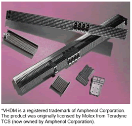 Teradyne Connector Systems changed the value formula by designing the VHDM (very-high-density metric) connector family with ground planes in mind. Its team basically stamped and overmolded a ground-plane wafer and lead-frame wafer and then married them to make one shielded wafer that was then stitched onto stiffeners to make large connectors. This approach had several benefits:
- The whole process could be done reel to reel, making it highly automatable and cost-effective.
- All the contacts could then be used for signals, effectively doubling density as compared to open-pin-field connectors.
- The wafer pitch was 2mm so no signal density was sacrificed for the ground planes.
- The team made wafers with more pairs – up to four pairs per wafer.
- Impedance control was dramatically improved.
- Crosstalk between wafers was dramatically reduced.
- Ground planes in the backplane header carried the ground connection between the daughtercard and backplane.
- Signals were not dedicated so customers could map high-speed pairs and/or low-speed signals anywhere on the connector.
- This connector was delivered on a stiffener with the exact number of signal, ground, power, and guidance modules needed.
The density and speed improvements were quite appealing to the high-end computing, internetworking, and instrumentation customers of the day, enabling TCS and Molex, its second source, to dominate high-end designs for several years. Lower-cost open-pin-field designs offered by competitors continued to dominate the telecom applications.
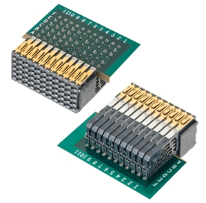
VHDM wafers are made with two over-molded lead frames that are married together to make one wafer. (Illustration from Molex)
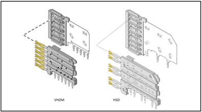
The very creative and productive engineering team at TCS, including Dave McNamara, Dan Provencher, Phil Stokoe, William Howard, and Mark Gailus, proved that, sometimes, being first is not as good as being the best at implementing an improvement like ground planes between wafers. The team continued to innovate grounding concepts through several generations of connectors (VHDM, HSD, and GbX) each time improving impedance control and reducing crosstalk. VHDM HSD (high-speed differential), for example, introduced the concept of dedicated differential pairs within the wafer with a ground contact separating pairs. The major improvement in the HSD design was in the PCB footprint. VHDM had a staggered grid of ground contacts between the signal contact vias and required the traces to “squiggle” out, making the pair loosely coupled. The HSD design committed every third pin to ground, allowing TCS to bring the ground contact vias in line with the signal contacts. This opened up a wide routing channel between wafers, just right for routing differential traces on the backplane and daughtercards. This improvement bumped the speed up to 6.25Gb/s, state-of-the-art for 1997.
So, to retrace the steps, first we had open-pin-field connectors with up to six rows that ran about 1Gb/s. Then additional shielding, especially with ground planes between wafers, enabled the speed to jump to 3.125Gb/s. Introducing differential construction and improved routing initially offered 6.25Gb/s. And while Teradyne was having so much fun with waferized, shielded connectors on long stiffeners, AMP and FCI were making larger open-pin-field designs, also using 2mm pitch.
Robinson Nugent (now 3M) UHM 2mm HM with fully shielded wafers.
Robinson Nugent (RN) was firmly dedicated to making a higher-speed 2mm HM connector. RN wanted full compatibility with existing Z-pack 2mm HM headers so that customers could upgrade systems with new daughtercards. It added shields between wafers and also shields between rows, creating boxes around each differential pair. RN was acquired by 3M, which still offers this high-performance hard-metric connector. The RN inventors include Sam Ramey, Kevin Meredith, Alexander Barr, and Jan Kusters.
The TCS strategy of empowering its engineering team to continuously develop better families of connectors enabled it to sell successive licenses to Molex for HDM, VHDM, and HSD. It developed a lot of customer loyalty and was able to command premium prices for each system because each was the fastest system available; this allowed customers to design forward-looking systems with connector capabilities that exceeded the speed of the chips available at the time.
Cross-section of Amphenol-TCS GbX connectors showing boxes created with intersecting ground planes
The next performance target was 10Gb/s. To achieve these speeds, connectors needed to have even lower crosstalk and more tightly controlled impedance. The TCS SI team advised that the way to tighten up impedance was to use a two-shot molding process. The signal lead frame was stamped and overmolded as before. The ground plane was married to the signal wafer then overmolded in a second molding pass. This process tightened up the tolerance of the position of the ground plane relative to the signal contacts and is done reel to reel. To increase density, TCS decreased the wafer pitch from 2mm to 1.85 and added another pair, delivering up to five pairs per wafer.
It should be acknowledged that the process development team was extremely important in accomplishing this. As the wafers became larger, it became increasingly challenging to keep them flat and perpendicular to the boards. The previous article in this series highlighted the importance of the stiffener in eliminating any tolerance buildup as the connector length grew to 18″ or more in length. Since each wafer was individually positioned into slots on the stiffener, the true position of the whole array was determined by the stiffener, a dimension tightly controlled in a simple stiffener-stamping die. To achieve the tighter wafer-to-wafer pitch and to reduce reflections from the plated through-hole, GbX used smaller, compliant press-fit pins to fit 0.018″ plated through-holes. Additionally, they oriented the backplane shields length-wise in the backplane header, simplifying, reducing cost, and creating partial ground boxes around differential pairs. The right-angle receptacle has ground planes between columns and is referred to as north-south. The backplane header has ground planes running east-west.
This series of inventions and refinements from the design team at Teradyne Connector Systems enabled the company to dominate high-end computer and internetworking applications for more than five years during the most intensively innovative time in backplane connector history.
Great Connector Inventions: Connector “Chicklets” Revolutionize Backplanes