Silicon Photonics – Are We Past the Hype?
From its inception, silicon/CMOS photonics was supposed to revolutionize optical communications, but has yet to come to fruition. How much progress has been made so far?
Both Intel and Luxtera have been working on silicon/CMOS photonics for more than 13 years. While we have a few products, its promise of lower-cost, lower-power-consumption optical devices that would revolutionize the industry has yet to come to fruition. Let’s look at some of the progress that has been made.
Silicon/CMOS photonics has several different implementations. Shown below is Intel’s, which is a hybrid in that it uses InP lasers to produce the light and silicon waveguides to direct it.
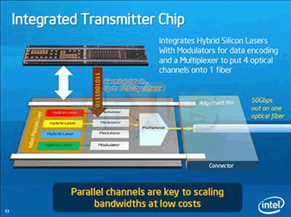
Intel’s CMOS Photonics (Source: Intel)
This image shows how the transmitter chip can then be integrated with modulators and multiplexers for four-channel operation. Intel’s program had a major setback in early 2015 when its original production run of modules did not meet specifications. New devices now are slated for production in early 2016.
While Intel was one of the first to start research and development on silicon photonics, Luxtera was the first to release products. Its devices have been available for more than nine years and are currently being used by Molex to supply AOCs to both the Ethernet and InfiniBand markets. Luxtera refers to its technology as “CMOS Photonics,” and it is based on the 1490nm wavelength range. In 2012, STMicroelectronics collaborated with Luxtera to help enable the high-volume market for silicon photonics. STMicroelectronics’ first devices, released in early 2015, were optical engines for the PSM4 version of the QSFP28 100G optical transceiver.
SiPh Value Chain
The chart below shows all of the companies involved in the silicon photonics value chain. They range from research and development to total systems, and some of these companies have moved up the value chain; Kotura, Caliopia, and LightWire were all acquired by equipment companies – Kotura by Mellanox, Caliopa by Huawei, and LightWire by Cisco (which may have prompted the first two).
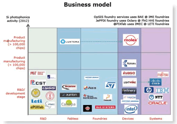
Silicon photonics value chain (Source: Yole Development)
There is a clear trend here for system companies to take control of their own future when it comes to silicon photonics. It may be in response to the whole idea of disaggregated racks from the open compute platform or because they realize that this technology can solve their chip-to-chip communications issues. Either way, it looks like the technology is becoming more and more prevalent. With seven foundries that can support production, silicon photonics is well on its way to mainstream adoption.
While this chart shows Infinera under the devices category, we believe it should be under the systems heading since all of its photonic integrated circuit (PIC) devices are consumed entirely in its own equipment. In fact, Infinera is probably the most successful silicon photonics company to date, with revenue of $668 million in 2014, up 11% over 2013.
What About Copper and VCSELs?
The chart below, which was presented at a Photonics 21 WG6 workshop, shows how “copper communications are approaching their intrinsic limits” and how “hybrid 2D and 3D photonics can’t meet the long term requirements.” With data rates increasing beyond 10G, chip-to-chip, on-board, and board-to-board optical interconnects will become progressively more significant.
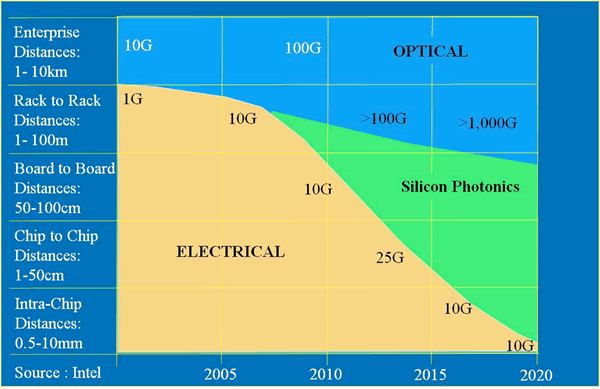
SiPh versus copper and traditional optics (Source: Photonics 21, WG6 Workshop, 2013)
Even at 10G, traditional printed-circuit boards cannot support transmission beyond about 12 inches without needing re-timers. While this chart shows the technical niche that silicon photonics can fill, another dimension where the technology seems to outperform traditional optics is in cost. According to Intel, its silicon photonics solution for all distances, from intra-chip through rack-to-rack, will get to less than $1 per Gb/s, which is an order of magnitude lower than existing long-reach optical solutions and almost on par with both short-reach optical (VCSEL-based) and copper ones.
Intel has taken it a step further. The microprocessor giant is now advocating that silicon photonics can enable the separation of computing devices. In other words, separate trays within a rack for compute, storage, and networking. Intel is collaborating with Facebook in order to make this a reality. It was demonstrated at the Open Compute Summit and continues to evolve.
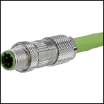
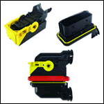
In addition, there are many other companies already using silicon photonics technology to sell AOCs and modules into the existing 40G and 100G Ethernet and InfiniBand markets. Some of these devices are pictured below.
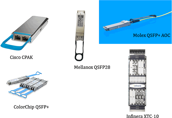
Above are several products that use silicon photonics. The Cisco CPAK is a form factor used for 100 Gigabit Ethernet. Cisco, along with other OEMs, was pushing for a smaller form factor than the CFP, which prompted the CFP2 and CFP4 MSAs. However, the timelines to get to production of these form factors was too long, and the power consumption of these modules was too high, so Cisco decided to take the leap into silicon photonics.
Mellanox was one of the first companies to release a QSFP28, largely because it was using its own silicon photonics (via its Kotura acquisition) to develop it. Molex and ColorChip both have QSFP+ products that use silicon photonics. Molex leverages Luxtera’s devices, while ColorChip has its own. Infinera’s DTN-X platform leverages its PIC technology to reach 1Tb/s slots.
Another illustration from the Photonics 21 WG6 workshop shows the timeline for silicon photonics adoption. The product portfolio is clear. We started with AOCs, moved into modules and backplanes, and the next steps will be interposers and opto-boards.
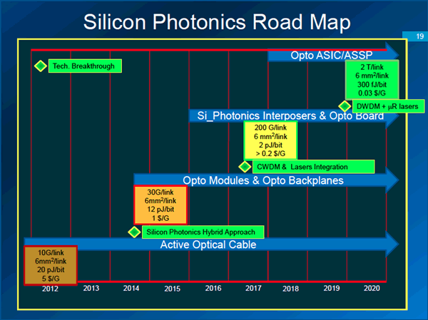
(Credit: Photonics 21 – WG6 Workshop, STMicroelectronics Contribution, 2013)
This shows that the hybrid approach has been adopted as, perhaps, an interim approach, but some believe the next hurdle may be insurmountable – silicon lasers. The reason we use GaAs (VCSELs) and InP (DFBs) for lasers is because these materials can be used to build reliable light-emitting devices. While silicon lasers have been demonstrated, researchers have yet to figure out how to make them reliable or be certain they can commercialize them. Even if silicon lasers do not materialize for quite some time, the cost and power consumption of the hybrid approach rivals that of any VCSEL or copper solution.
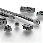
What does all of this mean to the connector industry? More optical devices, even on board, so we will see the slow elimination of electrical board-mount connectors in servers and switches. These will shift to optical connectors like MXC and Prizm LightTurn.