Porosity: Real World Concerns
Porosity: Real World Concerns
When I entered the connector industry in the early 1960s, porosity was the hot topic. During that period, gold thickness was at 100-200 microinches. As the plating process became efficient, porosity became a non-issue until the mid-’60s, when 50 microinches became the standard. Then porosity was hot again. This cycle has continued to repeat itself as gold plating thicknesses continue to diminish.
So what is porosity and why the concern? Porosity is microscopic discontinuities in the plating that cannot be seen by the naked eye. Extreme high magnification is required to view porosity, but these tiny inconsistencies can cause big problems.
Porosity originates during the manufacturing process and is due to:
- Substrate surface defects
- Unclean plating solutions
- Internal stressed deposits (micro cracks)
- Thickness of gold and/or nickel plating
- Process variables
- Improper underplating
In addition to the gold plating process, the use of a nickel underplate is also an important feature in the control of porosity. The following underplate features should be considered:
- A thickness of 100-150 microinches is ideal.
- A thickness of 50 microinches is acceptable but could also promote porosity to a small degree.
- A nickel thickness of less than 50 microinches can result in significantly increased porosity.
- The nickel underplate should be stress-free and ductile. High stresses in an underplate can result in cracking, leading to defects in the gold plating.
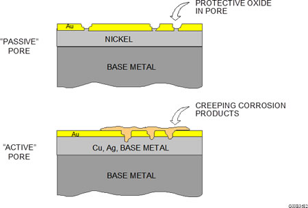
Figure 1: Passive and active pore sites
With respect to performance, there are two basic types of porosity, passive and active, as illustrated in Figure 1.
A passive pore is one in which the discontinuity is through the gold to the nickel underplate only. The nickel will form a nickel oxide film, which is self-limiting in thickness and is passive with respect to corrosion. In this case, the nickel oxide performs in the same manner as passivation of stainless steel. Assuming that the gold thickness is greater than 30 microinches, a contact that comes to rest on a pore site will not contact the exposed nickel and will not cause a fault.
An active pore is one where the discontinuity descends through the gold and the nickel, exposing the base metal, which is usually a copper alloy. The base metal will start to corrode and extend through the pore channel to the contact surface. Contingent on the corrosion products caused by the application environment, the contamination may start to creep across the gold surface and the probability of field failures will increase. This is the main concern. Porosity is not a laboratory phenomenon; it’s a real world concern.
Part of the concern is that pore corrosion is time-dependent. Porosity has caused field problems in as little as a few weeks and as long as years down the line, dependent on the application environment and performance requirements.
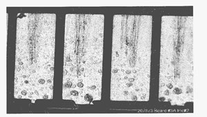
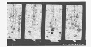
Figure 2. Pore corrosion sites on a PCB that failed in the field.
Pore sites occur randomly. Figure 2 shows pore corrosion on a PCB that failed in the field as a result of pore corrosion.
One pore in the wrong position can result in a circuit fault. Pore sites away from the contact area will not, in all probability, cause a fault, except in extreme cases of corrosion creep or migration.
The number of pores increases significantly as the gold and/or nickel thickness decreases. The effects of porosity may be controlled at gold thicknesses greater than 30 microinches with the use of pore blockers. For gold thicknesses of less than 30 microinches, porosity can increase significantly. With gold thicknesses of less than 10 microinches, it’s no longer an issue of pores, but instead a lack of surface coverage, which results in large areas without gold plating. Figure 3 shows a gold-flash contact where copper was exposed and corrosion creep covered the total contact surface.
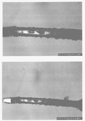
Figure 3. Surface corrosion due to incomplete surface coverage of a gold-flashed contact.
Porosity can be detected by use of EIA-364-TP53. This test procedure uses nitric acid vapor to define the pore sites. TP53 also defines the areas that require controlled porosity for a number of contact geometries.
Consider the question: Can thin gold be used? The answer is yes, but with a great deal of care. It can be used in application-specific situations. Thin gold should not be used when durability requirements include more than 10 mating cycles; when fretting is a problem; or when direct exposure to a harsh environment is involved. Sheltering of the connector system is essential. Anticipated field life is short.
The importance of this subject is increasing as the use of thin gold increases. It is a time-dependent phenomenon, and as a result, I have modified Peel’s Law: “Those who manufacture, sell, or buy thin gold-flash systems without proper application analysis deserve every problem that may result.”
By Max Peel, Senior Fellow, Contech Research
- Nanocrystalline Silver Alloy Contact Finishes in Electronic Applications - April 6, 2015
- Nanocrystalline Silver Contact Platings - March 16, 2015
- Dr. Bob on Gold Flash Contact Finishes (and Max Peel) - September 22, 2014