Electronic Connectors Shrink to Fit
Incredible advances in processor and memory technology have mandated shrinking all other electronic components from chip capacitors to connectors and the circuitry that joins them. The connector industry has responded to these challenges by introducing new classes of high-density microminiature connectors.
A basic pillar of the electronics industry has been its ability to stuff more functionality in less space. The ubiquitous smartphone now packs more computing power than a room-sized computer of the 1970s. According to Bell’s Law, a new, lower-price class of computing devices emerges roughly every 10 years. We have Moore’s Law and a continuing string of advances in technology to thank for the incredible growth of the mobile products we take for granted today. We have been conditioned to expect next-generation electronic products to be smaller, faster, and cheaper.
Incredible advances in processor and memory technology have mandated shrinking all other electronic components from chip capacitors to connectors and the circuitry that joins them. Printed circuit board traces and spaces have shrunk, requiring component suppliers to reduce contact centerlines. Through-hole PCB attachment has been supplemented with surface-mount, ball-grid, pin-grid, and land-grid technology. Compliant press-fit pins have shrunk to fit into smaller plated through-holes. At the same time, connector pin counts continue to rise.
A combination of physics, economics, and marketing is driving the demand for ever-smaller separable interfaces:
- The explosion of mobile products dictates smaller and lighter devices.
- Demand for faster circuitry results in signal distortion that gets worse as the length of the circuit increases. Shorter device-to-device links become preferable.
- Smaller products have minimal space for internal or external interconnects.
- The ability to build cost-competitive products favors standardized commodity interfaces.
Requirements for tighter packaging generate a whole new set of design challenges:
- High-speed signals in close proximity suffer from signal degradation due to crosstalk.
- Increased number of input/output lines must compete for scarce I/O panel space.
- Packing more components into less space can create major thermal problems.
- Miniaturized connectors and contacts may be more fragile, yet must survive in tough consumer applications.
- Smaller contacts typically have lower current ratings.
- Cost-reduction efforts minimize the number of separable connectors in devices that are rarely repaired. Connectors may be limited to interfaces required by the manufacturing process.
The electronics product industry has been downsizing its selection of connectors for the past 10 years: Apple Computer replaced its 30-pin docking connector with the eight-pin Lightning I/O connector in 2012 to allow further envelope reduction of its mobile products, among other reasons; the USB interface has evolved to include standard, mini, and micro configurations to enable use on ever-smaller devices; the new M.2 PCIe mini card connector consumes 20% less PCB space than prior internal mini-card connectors and facilitates the expansion of solid-state disk drives.
The connector industry is responding to these challenges by introducing new classes of high-density microminiature connectors. In an effort to create high-speed, small centerline interfaces that are cost-effective, many of these new connectors utilize simple beam-on-pad interfaces similar to a card-edge connector.
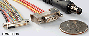 Bob Stanton, director of technology at Omnetics, a company that specializes in miniaturized connectors, identified several trends that currently are shaping the miniature connector industry. He sees emerging applications for tiny interconnects including flex ribbon cable in robotic, surveillance, and medical device markets. In an effort to conserve space, shell-less post and receptacle connectors are being used with custom signal and ground patterns to support high-speed circuits. Omnetics has created a manufacturing process that can quickly model and build custom configurations of mixed-signal connectors to satisfy highly specific signal and power requirements from customers.
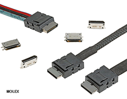 Larger, more diversified connector manufacturers are responding to demands for more space-efficient interfaces to address broad market applications. Molex released its new Nano-Pitch I/O interconnect system that combines a tiny 5mm high x 15mm wide x 9mm deep profile with up to 24Gb/s per-lane performance capable of supporting multiple industry standards.
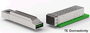 QSFP and QSFP28 pluggable I/O connectors have become the de facto standard in high-density data communications and networking applications. As the struggle for shrinking I/O panel space continues, TE Connectivity and others have introduced the Micro QSFP in support of next-generation equipment. Designed to support 50Gb/s PAM-4 signaling, these new connectors offer 33% panel density improvement. The new micro QSFP specification, as defined by the µQSFP Multi Source Agreement (MSA), will ensure mechanical and electrical compatibility among competitive suppliers.
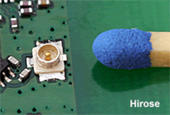 Mobile consumer products continue to shrink in size while expanding capabilities. These devices connect to the outside world via Wi-Fi, cellular, Bluetooth, and NFC wireless links, which often require management of RF signals. Microminiature RF connectors that offer a mated profile of only 1.0mm provide one of the few separable interfaces utilized in these devices.
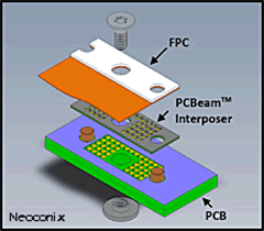 System packaging engineers continue to search for products that consume as little space as possible. Taking a cue from land-grid array technology, the Neoconix PCBeam interposer offers fine-pitch, high-speed, and high-pin-count interconnects. Board-to-board and semiconductor socket arrays feature contacts on 1.27mm, 1.0mm, 0.8mm, and 0.74mm centerlines, with stacked heights of only 0.23mm. Neoconix and Samtec have established a technology licensing agreement that ensures dual sourcing for this unique high-density interface.
It is likely that the race to higher-speed system packaging density and demand for stringent signal integrity will eventually migrate many interconnects to fiber optic alternatives. Optical interfaces offer nearly unlimited bandwidth, much-reduced size and weight, and the ability to create long channels with minimal distortion. Taking advantage of expanded-beam technology, the recently introduced MXC connector illustrates the advantage of fiber optics with a connector envelope of only 13.65mm x 4.75mm, while linking up to 64 optical fibers.
It is hard to predict where the demand for miniaturization will take us. Discrete components are being replaced by system-on-package and system-on-chip packaging. Microelectromechanical systems (MEMS) are well past the development stage. Researchers are exploring the properties of graphene and have already demonstrated self-assembling electronic circuits using nanotubes. Traditional stamped and formed contacts will not work on that scale.
The Internet of Things (IoT) is expected to require billions of tiny devices linked to the Internet. Electronic products utilizing monolithic modules that communicate via radio or optical links could be the next evolution of remote and mobile devices, potentially squeezing out separable copper connectors as we know them today.


- XPO, Addressing the I/O Panel Bottleneck - June 30, 2026
- Agentic and Neuromorphic Computers Enable the Future of Digital Computing - May 26, 2026
- OFC 2026: High-Speed Networking in the AI Era - April 7, 2026