High-Speed Signals Take the High Road
Very early computers were a mass of discrete point-to-point wires. The combination of physics and economics is bringing that interconnect architecture back full circle.
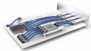
Samtec’s flyover systems harken back to, but improve upon early interconnect architectures. (Image courtesy of Samtec, Inc.)
Design engineers have been grappling for years with the challenge of propagating ever-increasing signal rates in printed circuit boards. As data rates pushed into RF regions, signal modeling transitioned from simple DC resistance to transmission lines that exhibit a whole new set of characteristics. Factors including impedance, attenuation, crosstalk, skew, jitter, intersymbol interference, and reflections all influence required signal integrity of the channel and must be managed. Each incremental boost in system bandwidth necessitates a complete analysis of the entire channel, from source to destination. In spite of predications of the practical performance limitations of copper conductors, engineers continue to find ways to push multilayer PCB technology to new heights.
Upgraded versions of traditional FR-4 PCB laminate material offer lower losses via reduced dielectric constant (Dk) and dissipation factor (Df), along with improved mechanical properties. Tight control of thickness, copper surface roughness, coefficient of thermal expansion, and the degree of moisture absorption are now specified characteristics. More exotic laminate materials are the gold standard for high-end performance, but these come with a significant increase in cost.
As board layer counts increase and feature dimensions shrink, PCB fabrication processes have been modified to add backdrilling of plated through-holes (PTHs) to minimize the effect of stubs. System engineers adopted a new set of layout rules to minimize crosstalk, skew, and attenuation. The transition between a connector and the PCB was recognized as being a major source of signal distortion. In response, connector manufacturers began providing detailed launch footprint design guides for their high-performance connectors. The use of channel, modeling, simulation and verification, eye diagrams, and S-Parameter data have become standard practice.
The design of high-performance backplane connectors continues to evolve. Grid-based contact patterns have been optimized for differential pair signaling, and the signal path through the connector body has been modified to minimize skew and impedance discontinuities. Some suppliers also adopted the use of multiple dielectric materials with specific properties, as well as air, to improve performance. The size of compliant pins was reduced to allow smaller PTHs.
Software conditioning of high-speed signals enabled the reliable discrimination of low-level signals once thought impossible to detect. Advanced features such as equalization, compensation, and forward error correction have kept copper alive well past its anticipated demise.
All of these channel improvements are focused on maintaining the ability to design circuits of required length with standard bit error rates (BERs) and acceptable costs. Optimizing system design must consist of a delicate balance between increasing signal frequency, channel length, loss budget, and, ultimately, cost.
System architects are now considering an alternate approach that reduces the use of PCB traces to conduct high-speed signals.
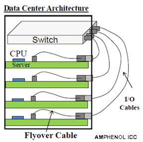 Rather than routing the highest speed signals through multiple layers of a high performance PCB, signals are transferred to shielded differential pair cable where impedance can be better controlled and signals are isolated from external noise and crosstalk. A connector is located immediately adjacent to an FPGA or processor, which launches the signals out of the PCB where they “fly” over the board via discrete or ribbon twinax cable to another location on the board, or to an I/O connector.
The PCB continues to conduct low- to medium-speed signals as well as power. Current applications may fly only a select number of high-speed lines, typically 16 to 24 pairs. By eliminating high-speed PCB traces, the complexity and cost of the board can be much reduced. eliminates Expensive hand routing is eliminated and layer count minimized. The need for signal conditioning features may be reduced or even eliminated.
As signal speeds increase, the practical length of a PCB-etched conductor becomes shorter. For instance, at 56Gb/s, signal degradation can become unacceptable in channels as short as 10”. Use of the flyover concept may well become the most cost-effective solution at lengths much beyond that point. Discrete twinax cable has been optimized with multiple conductor sizes and advanced shielding to the point that flyover may become the only practical solution in larger systems with long channels.
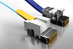 Samtec originated the flyover concept several years ago with their Firefly™ Micro Flyover System™, which consists of both copper and optical components in an expanding array of interface options, including their flyover QSFP.
Since then, other major connector manufacturers have introduced products that take high-speed signals out of the board. The cable backplane is another example of a solution designed for situations in which long channels, increased data rates, and signal integrity are pushing designers to find new ways to manage these signals.
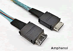
Amphenol features a collection of internal PCB-to-cable connectors, including OCuLink, which can fly signals to a high-performance backplane connector or to a Mini SAS HD panel-mount connector.
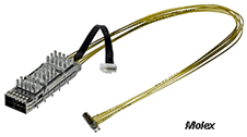
Molex’s new BiPass I/O connector provides a flyover link to a ZQSFP pluggable interface.
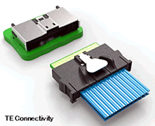
TE Connectivity beefed up its low-profile internal connector line with the Sliver PCB connector, which is ideal for flyover applications.
Each of these suppliers utilize internal precision cable manufacturing and assembly resources to assure repeatable reliability. The flyover design harkens back to the early days of computers with its mass of discrete point-to-point wires, and is poised to bring that bygone interconnect architecture back full circle to satisfy both the physics and economic mandates of advanced high-speed system design.

Recently posted:
[related_posts limit=”10″]

- Agentic and Neuromorphic Computers Enable the Future of Digital Computing - May 26, 2026
- OFC 2026: High-Speed Networking in the AI Era - April 7, 2026
- DesignCon 2026 - March 17, 2026