Moore’s Law after 50 Years
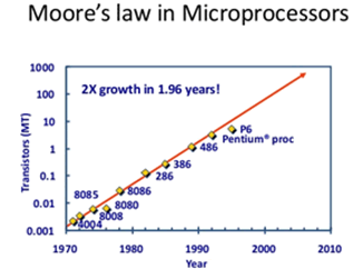
It is unclear if Gordon Moore realized what a powerful challenge he created over 50 years ago with his famous theorem. His forecast that the number of transistors in a given space will double every two years set the stage for the development of the incredible computing power that we utilize in a universe of electronic devices today.
To a large degree, Moore’s Law is all about economics. The basic manufacturing cost of a semiconductor device depends of the number of transistors that can be crammed on each chip. Semiconductor dies are fabricated on thin wafers of pure silicon. A smaller chip results in a higher yield per wafer, which translates to lower cost per chip. Increasing the number of transistors on the same size die can deliver more features or computing power, which can translate to a higher sales price per die. Much more than a simple prediction of technology development, Moore’s Law provides a roadmap to dramatically reduce cost per computing cycle. To a limit, smaller transistors are also able to switch faster and use less power.
 For many years, the industry increased both transistor density and switching speed to satisfy increasing application demands. That worked well until the turn of the century, when high-speed transistors in very close proximity consumed more power and generated excessive heat. If left unchecked, this dramatically reduced the reliability and life of the device. Low power consumption became a critical issue as mobile devices that rely on battery power began to dominate the consumer market. The answer came in the form of multi-core processors where tasks are allocated among several lower speed processors and advanced software that shuts down unneeded functions to reduce power. The first Intel two-core processor, introduced in 2008, featured 410 million transistors with a bus speed of 1066 MHz. Intel’s Horse Ridge II, released in late 2020, is a quantum computer with the ability to manipulate and read qubit states and control the potential of several gates required to entangle multiple qubits.
Multicore processors continued the drive to further reduce transistor dimensions. Spacing between features on chips is expressed in nanometers, which is one billionth of a meter (0.000000001 m). A human hair is 80,000 to 100,000nm in diameter. Advanced chip-manufacturing processes evolved over the years from 130nm to 90nm to 65nm to 45nm to 2nm.
Staying on track to maintain the pace of Moore’s Law has been neither cheap nor easy. Achieving these remarkable advances raised serious technical challenges, including increased leakage current, which is power consumed even when the device is idle. The cost of building a semiconductor production facility capable of producing chips with the smallest feature dimensions may now top $1 billion.
Some industry pundits have begun to question the ability to continue doubling the density of chips. Certainly there are finite limits on how small individual features can be created on silicon chips. Research on gates consisting of individual atoms may provide a long-term roadmap, but in the shorter term, industry leaders have introduced new architectures that will extend the current pace of functionality per square mm.
System-on-chip architecture is expanding the capability to increase device functionality by integrating multiple functions on a single chip. Transistors and memory have co-existed in microprocessors for many years, but designers are now integrating key system building blocks, including analog/RF, power, sensors, and even biochips on a single silicon chip. Field programmable gate arrays (FPGAs), for instance, are designed around a multiple block architecture that consists of programmable logic, switch and I/O blocks. Programmable links between these blocks makes them easily adaptable to a wide range of applications. They have become key components in equipment that ranges across applications and industries, from automotive to aerospace.
The Holy Grail in the high-speed data transmission arena today would be the ability to add photonic laser transmitters and optical receivers directly on silicon. Integrated chips at this level could drastically reduce the size, weight, power consumption, and cost of electronic devices, many of which will be part of the Internet of things.
Another solution to increasing the performance and density of a chip is through the adoption of 3-D topography. As the density on a single plane reaches a practical limit, it makes sense to start building vertical structures on the surface of the die. Intel Tri-Gate transistors offer significant transistor density and performance improvements over traditional planar technology.
Processors as well as memory devices are now being manufactured using this 3-D design.
In devices that simply cannot be shrunk, the industry has adopted stacked memory technology. Multiple layers of high density memory can be located much closer to a processor, reducing signal delay.
At this point, it appears that Moore’s Law will continue to be the yardstick that gauges the progression of increased computing power at lower cost. Greg McSorley, business development manager, High-Speed Interconnects at Amphenol, said the exact number of transistors per square mm and the time periods between generations may be altered somewhat, but the concept of Moore’s Law is still valid and will continue to be a useful guide in the future.

- XPO, Addressing the I/O Panel Bottleneck - June 30, 2026
- Agentic and Neuromorphic Computers Enable the Future of Digital Computing - May 26, 2026
- OFC 2026: High-Speed Networking in the AI Era - April 7, 2026
