Nanocrystalline Silver Contact Platings
New silver alloys address the issues of durability and conductivity through a fundamental difference in crystalline structure. Dr. Bob takes a closer look at nanocrystalline silver contact platings.
 Two papers* were published last year that introduced nanocrystalline silver alloy contact platings – one a silver-palladium alloy and the other silver-tungsten. Both papers cite the potential for these platings as alternatives to gold/nickel finishes in electronic connector applications. Here, I will limit my remarks to one of those applications – power contacts/connectors – where silver platings are already in common use.
Silver is used in power applications because of its high electrical conductivity and better arcing resistance than gold or tin. It does have limitations, however, in mating durability and mating force due to the requirement for high contact forces in power applications to enhance the magnitude and stability of contact interface resistance. These new silver alloys address these issues through a fundamental difference in crystalline structure – nanocrystallinity. That is, nanocrystalline silver has a smaller grain size than traditional silver contact finishes, which impacts both durability and conductivity.
My metallurgist core is delighted to have the opportunity to explain these differences as fundamentally due to the grain size of the materials. The following discussion is simplified, but basically correct. Conveniently, Table 1 (which is Table 2 of the silver-tungsten paper) contains the data needed to accomplish my task.
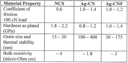
Table 1: Material Properties of Selected Silver Plating
The materials in Table 2 are nanocrystalline silver (NCS) and the currently used silver platings, Ag-CN (cyanide-plating bath) and Ag-CNF (a cyanide-free plating bath). The third row in the table presents the grain size data. The NCS grain size is significantly smaller than that of the other two finishes, in particular in the thermal stability of the grain size. Grain size typically increases with thermal exposure; the increase, of course, is dependent on the time at temperature. Two thermal aging exposures were used in the paper – 24 hours at 250°C and 1000 hours at 125°C. In both exposures, the NCS showed minimal grain coarsening; the Ag-CNF showed some coarsening; and the Ag-CN showed significant coarsening. The significance of minimal grain size coarsening is that the improvements in performance of the nanocrystalline silvers will have greater thermal stability.
Consider mechanical properties first. In metals, both the hardness and the yield strength depend on grain size. The reason for the dependence is due to the difference in grain boundary area with grain size. Small grains will have a larger grain boundary area for a given volume than larger grain sizes and grain boundaries, due to the disturbance in crystal structure across the boundary between grains; inhibit grain deformation kinetics; and, therefore, increase both the hardness and yield strength of the metal.
The relative hardness of the three silvers is shown in the second row of Table 1. The NCS is significantly harder than the other two silvers. Hardness, in turn, determines both the durability and coefficient of friction of the metal. Durability and mating wear resistance increase and the coefficient of friction decreases as hardness increases. The coefficient of friction for the three silvers is shown in the first row of Table 1. With that background, attention turns to power contacts and connectors.
Power Contacts and Connectors
As previously noted, in power contacts, contact force is a particularly important parameter because contact resistance decreases and contact resistance stability increases, with increasing contact force. Acting together, these two parameters reduce the Joule heating intrinsic to power applications and minimize the potential for thermal runaway due to contact resistance degradation over time in the field. So for electrical performance, high contact force is a plus of particular benefit in power applications.
The situation is the opposite for mechanical performance, in particular durability and mating force. Durability, as measured by the number of mating cycles that can be supported without performance degradation, decreases as contact force increases. The kinetics of wear may also change, with negative results, as contact force increases. Simply put, burnishing wear and low wear rates can transition to adhesive wear and high wear rates as contact force increases – a double whammy. These changes are primarily due to material hardness, with harder materials showing lower wear rates as noted above. Similarly, mating forces increase with increasing contact forces as well as with increasing coefficients of friction in the mating system.
These opposing electrical and mechanical dependencies dictate an optimization of the contact force to balance these effects. The first and second rows of Table 1 indicate that the CNF will, fundamentally, have better durability and mating characteristics than the current silvers due to higher hardness and lower coefficient of friction. This, in turn, allows the use of higher contact forces to enhance the electrical performance of the connector.
Electrical Performance
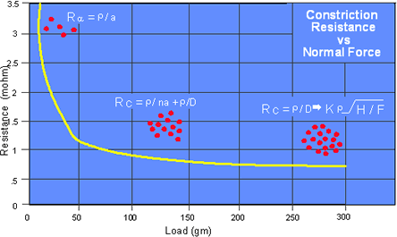
Figure 1. Contact Constriction Resistance vs. Contact Normal Force.
Consider now the electrical performance. Figure 1 shows the relationship between contact force and contact interface resistance (constriction resistance). The kinetics of this relationship are determined by the fact that on the micro-scale of the contact interface, all surfaces are rough. Note that at low contact forces only a few contact interfaces, called a-spots, will exist and occur where the high spots (asperities) of the two surfaces happen to come into contact. The formula for the resistance of an individual a-spot is shown as:
Ra = ρ/da
where Ra is the a-spot resistance, ρ is the electrical resistivity of the materials in contact (in connectors the contact finish), and da is the diameter of the a-spot. As the contact force increases, more asperities come into contact, increasing the number of a-spots and the resistance decreases because all the a-spots are electrically in parallel. The middle equation in Figure 1 indicates a series resistance. The series resistance is due to the initial constriction of the current flow in the contact beam to the distributional area of the a-spots, the ρ/D term, followed by the micro-constriction of the current through the individual a-spots, the ρ/nda term. The last equation in Figure 1 represents the resistance at high-contact forces when the multiple a-spot composite areas perform as though the contact area is a single contact area (SCA). At that point, the contact resistance is dominated by the distributional area of the a-spots and is given by:
Rc =ρ (H/FN)1/2
where Rc is the contact interface resistance, ρ is the resistivity of the contact beam material (where most of the constriction takes place), H is the hardness of the surface material (in most cases the contact finish where most of the contact interface deformation takes place), and FN is the contact normal force.
Note that the contact finish comes into play in two ways – electrically at the a-spots and mechanically at the SCA. As noted above, Ra, the resistance of an a-spot, depends on the resistivity of the finish (the first equation above). At the SCA (the second equation above), it is the resistivity of the contact spring base metal that is appropriate, because most of the current constriction will take place in the contact spring, and the hardness, H, of the finish because that is where the deformation takes place.
The fourth row of Table 2 shows the bulk electrical resistivity of the silver finishes. Note that the NCS finish has a higher resistivity than the other alloys. This, too, is a consequence of the nanocrystalline grain boundary area effect. The same crystal structure disturbance that results in the increase in hardness increases the electron scattering, which increases the electrical resistivity. This increased electrical resistivity will cause an increase in the a-spot series resistance term, which will, in turn, incrementally increase the contact interface resistance.
To sum up, the nanocrystalline silver platings discussed in these papers address the durability limitations of current silver platings and allow for the optimization of electrical and mechanical performance at higher levels of contact normal force. This, of course, enhances the contact/connector electrical performance – both magnitude and stability –which is of particular importance in power applications.
*The two papers referenced in this article are:
- “Connector Level Performance Evaluation of a New High-Speed Reel-to-Reel Electroplated Silver Palladium Alloy Contact Finish,” presented at ICEC 2014: The 27th International Conference on Electrical Contacts.
- “Performance Testing and Evaluation of a Ag-W Nano-Crystalline Silver Alloy as a Gold Replacement in Electrical Connectors,” presented at Holm 2014: 60th IEEE Holm Conference on Electrical Contacts.
- Nanocrystalline Silver Alloy Contact Finishes in Electronic Applications - April 6, 2015
- Nanocrystalline Silver Contact Platings - March 16, 2015
- Dr. Bob on Gold Flash Contact Finishes (and Max Peel) - September 22, 2014