Over-the-Board Technologies Raise High-Speed Signals to New Levels
Copper will reach its limits, but connector companies are pushing that day into the future with an exciting array of connectivity products that fly, jump, and pass over the board to increase performance.
Design engineers have been grappling for years with the challenges of propagating ever-increasing signal rates in printed circuit boards (PCBs). As data rates pushed into radio frequency (RF) regions, single-ended signaling transitioned to differential signaling. Channel modeling evolved from simple direct current (DC) resistance to transmission lines that exhibit a whole new set of characteristics. Factors including impedance, attenuation, crosstalk, skew, jitter, intersymbol interference, and reflections all influence the signal integrity of the channel and must be managed. Each incremental boost in system bandwidth necessitates a complete analysis of the entire channel, from source to destination. Despite predictions of the practical performance limitations of copper conductors, engineers have continued to find ways to push multilayer PCB technology to new heights.
Upgraded versions of traditional FR-4 PCB laminate material offers lower loss via reduced dielectric constant (Dk), dissipation factor (Df), and improved mechanical properties. Tight control of factors such as thickness, copper surface roughness, coefficient of thermal expansion, and degree of moisture absorption are now defined characteristics. Even tiny inconsistencies of the glass weave can degrade the signal. More exotic laminate materials, such as Megtron 6, became the gold standard for high-end performance but these materials come with a significant increase in cost.
Demand for isolation between high-speed signals embedded in the board resulted in layer counts increasing. PCB fabrication processes were modified to add back-drilling of plated through-holes (PTHs) to minimize the effect of stubs. System engineers adopted new layout rules to minimize crosstalk, skew, and attenuation. The transition between a connector and the PCB was recognized as being a major source of signal distortion. Connector manufacturers began providing detailed launch footprint reference design guides for their high-performance connectors. The signal path through the connector body was modified to minimize skew and impedance discontinuities. Some suppliers adopted the use of multiple dielectric materials with specific properties as well as air to improve performance. The size of compliant pins was reduced to allow smaller PTHs.
Signal conditioning functions built into serializer-deserializer (SerDes) devices enabled reliable discrimination of low-level signals previously thought impossible to detect. Advanced features such as equalization, compensation, and forward error correction have kept copper alive well past its anticipated limits. The recent industry migration from non-return-to-zero (NRZ) to PAM4 signaling has enabled 56+Gb/s channels without major changes in materials or fabrication processes.
These channel improvements are focused on maintaining the ability to design circuits of required length with acceptable bit error rates (BER). Optimizing system design consists of a delicate balance between increasing signal frequency, channel length, loss budget and, ultimately, cost.
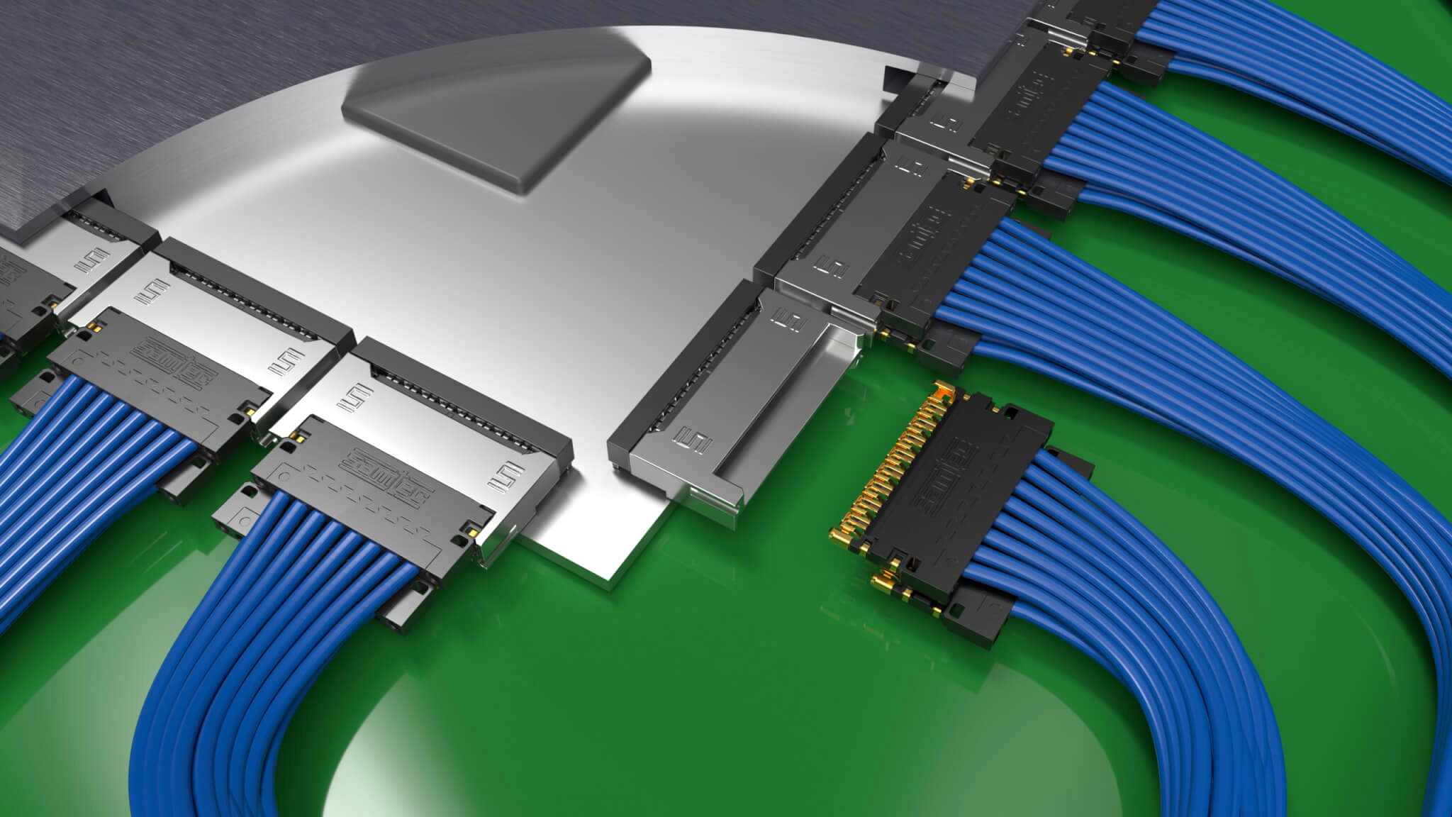
System architects have a new option that reduces the use of lossy PCB traces to conduct high-speed signals. Rather than routing the highest speed signals through multiple layers of high-performance PCB material, signals are transferred to shielded differential pair cable where impedance can be better controlled and signals are isolated from external noise and crosstalk. A copper or fiber optic connector is located immediately adjacent to a field-programmable gate array (FPGA) or processor, which launches the signals out of the PCB where they transmit over the board via discrete or ribbon twinax cable to another location on the board, or to an input/output (I/O) connector.
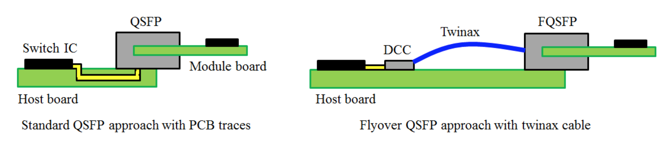
Diagram from Samtec’s DesignCon 2017 presentation, “Design of Flyover QSFP (FQSFP) for 56+Gb/s Applications”
The PCB continues to conduct low- to medium-speed signals as well as power, so a lower-cost laminate can be used. Current applications may fly only a select number of high-speed lines, typically 16 to 24 pairs. By eliminating high-speed PCB traces, the complexity and cost of the board can be much reduced. In addition, expensive hand routing is eliminated, layer count is minimized, and the need for signal conditioning features may be reduced or even eliminated.
As signal speeds increase, the practical length of a PCB-etched conductor becomes shorter. At 56Gb/s, signal degradation may become unacceptable in channels as short as 10”. Use of jump-over interconnect technology can significantly increase the effective length of a high-speed channel and may become the most cost-effective solution. Discrete twinax cable has been optimized with multiple conductor sizes and advanced shielding to the point that jump-over may become the only practical solution in larger systems with long channels.
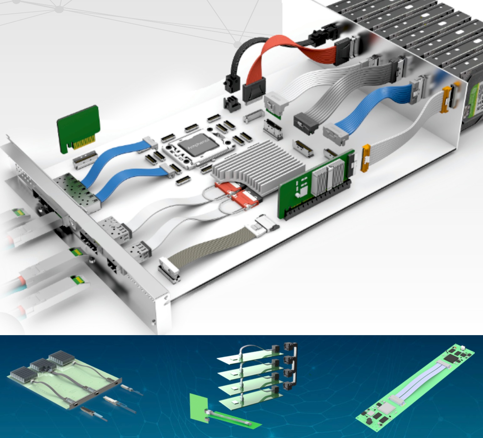
Samtec originated the Flyover concept several years ago with their FireFly Micro Flyover System, which consists of both copper mid-board connectors and optical transceiver assemblies in an expanding array of interface options. Both copper and optical cable assemblies mate with the same PCB-mounted headers.
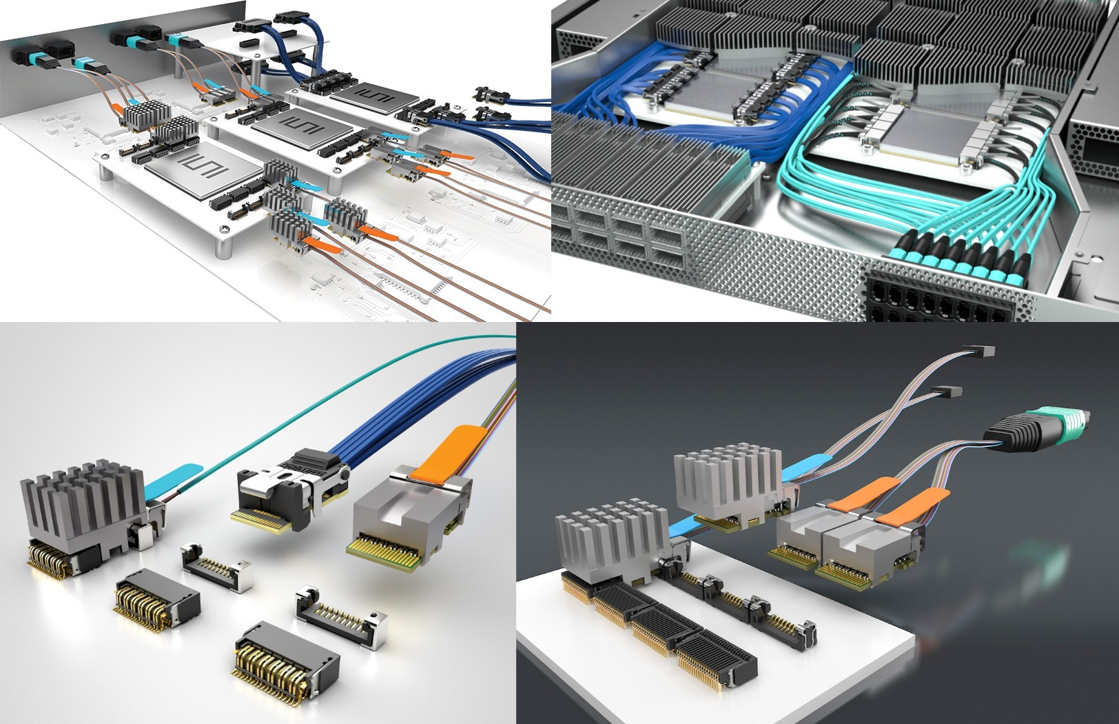
The FireFly family has expanded to enable a variety of board-to-board and board-to-I/O interconnects, including a board-to-QSFP connector.
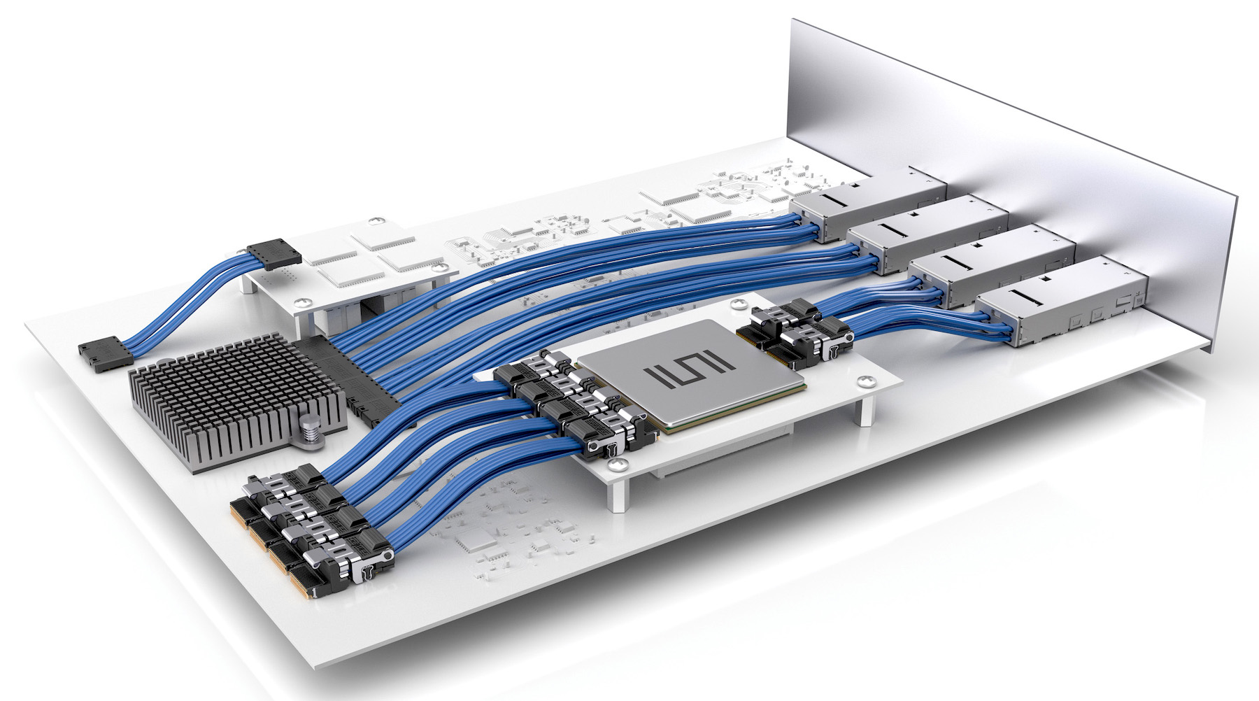
The latest addition is the Si-Fly, which is a direct cable-to-IC substrate or package interconnect. This high-density connector replaces the traditional ball grid array (BGA) connection to the PCB with a high-performance pluggable twinaxial cable rated to 112Gb/s PAM4.
Additional major connector manufacturers have introduced their own products that are designed to take high-speed signals out of the board.
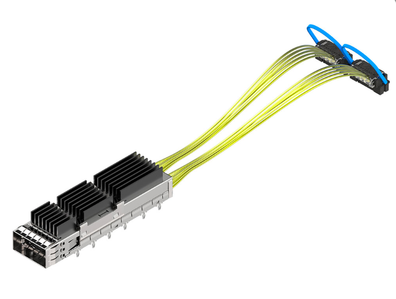
Amphenol ICC is expanding its line of internal OverPass cable products, including PCB-to-PCB, PCB-to-SFP, QSFP, and QSFP-DD I/O connectors. The most recent addition, the new LinkOVER compression cable connector, can run 112Gb/s PAM4 over one meter of cable.
Amphenol ICC’s OverPass cable assemblies
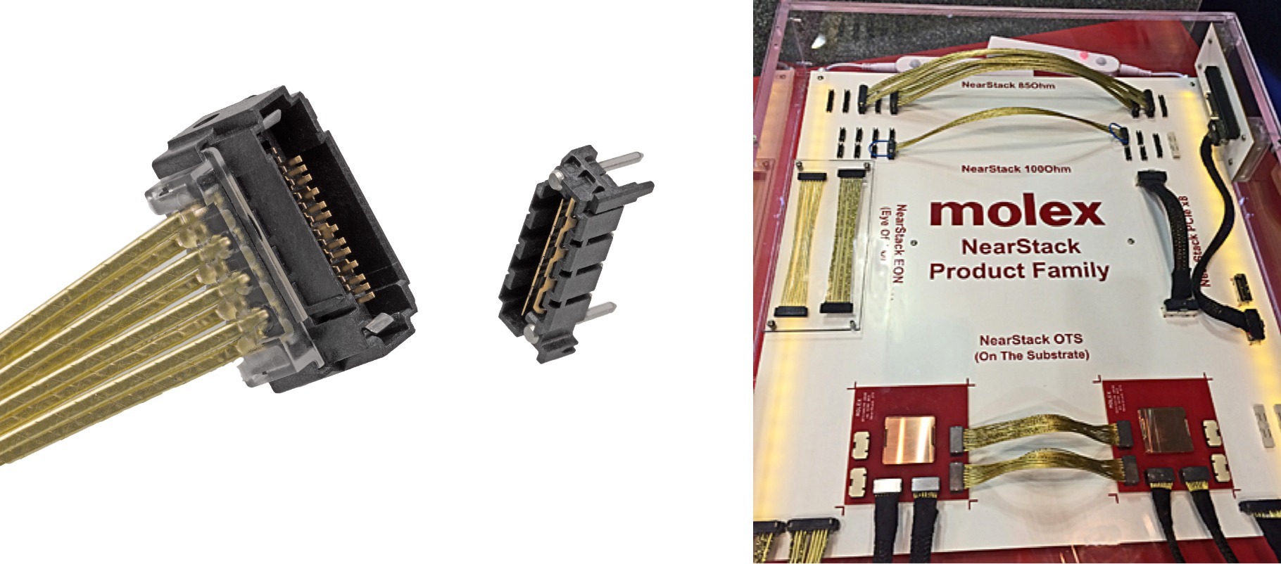
Molex offers the BiPass I/O connector, which provides a low-profile twinaxial copper link to a zQSFP pluggable interface.
The Molex NearStack connector family is based on a 0.6mm-pitch interface in a low-profile housing that can be used in multiple board-to-board applications. NearStack connectors are rated to 56Gb/s NRZ.
TE Connectivity’s low-profile internal connector line includes the Sliver PCB connector, which is ideal for jump-over applications. Sliver connectors have been adopted as the standard for SFF-TA-1002, which supports EDSFF, PCIe, and OCP NIC specifications.
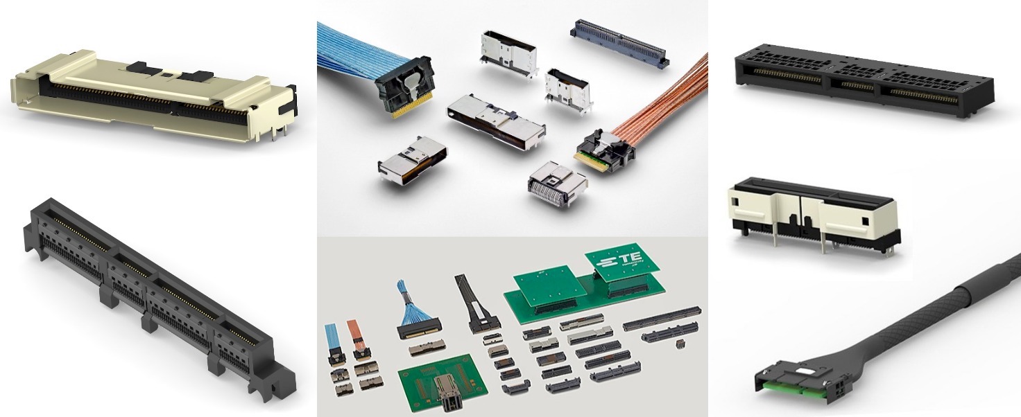
TE also offers a Strada Whisper cable assembly with a high-speed backplane connector at one end and a variety of mid-board connectors, such as Sliver or I/O connectors, at the far end.
Each of these suppliers utilize internal precision cable manufacturing and assembly resources to assure repeatable reliability.
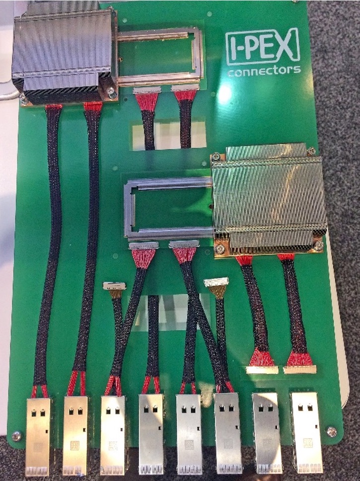
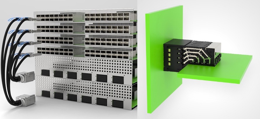
Many jump-over applications involve links from a processor or application-specific integrated circuit (ASIC) to the I/O connector. Connectors are mounted as close as possible to the device in order to reduce the length of PCB trace to a minimum. I-PEX specializes in manufacturing extreme high-density coaxial and twinaxial connectors. The company’s low-profile connectors are designed to fit under the heat sink of a processor to further reduce PCB trace lengths. The next anticipated step will be twinaxial connectors that mate directly to the device.
High-speed system designers are determined to continue using copper for as long as possible. Years of design experience, well established manufacturing processes, and low materials cost continue to drive this preference. Advanced signal conditioning, high-performance PCB materials, and adoption of PAM4 signaling are providing the migration path to 112Gb/s channels. Lifting the highest-speed signals out of the board to avoid material losses is one more tool system designers are using to push out the day when copper reaches the limits of physics and opens the door to much-delayed optical alternatives.
Like this article? Check out our other high-speed, RF and coax, and Connector Basics articles, our Datacom/Telecom and Wire/Cable Market Pages, and our 2020 and 2019 Article Archives.

- XPO, Addressing the I/O Panel Bottleneck - June 30, 2026
- Agentic and Neuromorphic Computers Enable the Future of Digital Computing - May 26, 2026
- OFC 2026: High-Speed Networking in the AI Era - April 7, 2026