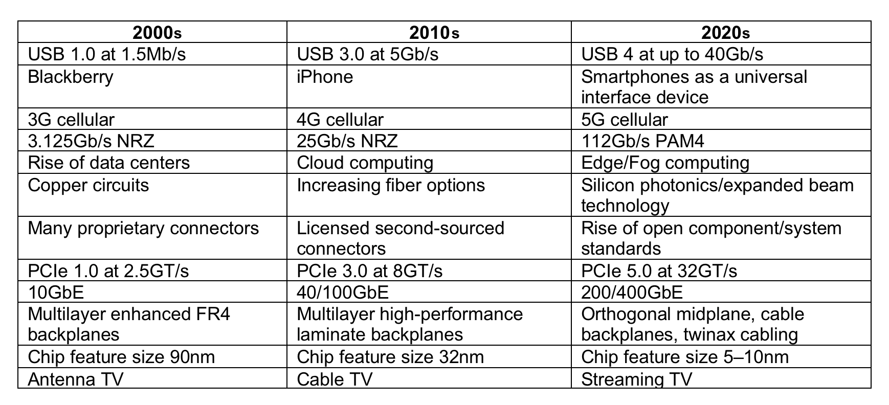
Top 12 Technology Trends: Copper to Optical Connectivity
This is the fifth installment in a series of articles that address leading technology trends that have had a significant impact on the electronic connector industry over the past 20 years.
This latest installment in the Technology Trends series by Bob Hult examines the trends and technologies that have pushed copper to the limits and ushered in fiber optic cables.
*Please note that the order of these 12 electronic product technologies is arbitrary, with no intent to indicate a level of relative importance.
Copper to Optical Connectivity
Copper conductors have served the connector industry well since the beginning of the electronics age. The unique qualities of copper, including excellent electrical and thermal conductivity, ductility, and availability, made it the natural choice for conducting circuits that range from milliwatt signal to kilowatt power.
Copper alloys, including beryllium copper and phosphor bronze, provide the required spring characteristics needed to ensure adequate normal force, and they can be formed into complex contact configurations using high-speed stamping dies. A variety of plating materials that range from gold to tin reduce contact resistance, increase durability, and prevent corrosion. Copper cables can be reliably terminated using a variety of techniques, including solder, crimp, insulation displacement, and welding. Copper circuits embedded in multilayer PCB laminate materials have enabled high-density connectivity between hundreds of devices mounted on the board. Components on these boards are attached using high-speed automated equipment and then mass terminated using process-controlled wave soldering equipment. Many years of designing and building reliable copper circuits have resulted in confidence in the medium, as well as a global supply chain of fully tooled contract manufacturers.
Copper is an excellent material, but it does have its limits. As system speeds continued to increase, copper conductors began to exhibit adverse characteristics. In addition to simple DC resistance, factors such as impedance variations, forward and backward crosstalk, skew, jitter, and inter-symbol interference tend to degrade the quality of a digital signal. Additionally, EMI and potential for ground loops must be addressed. Each of these negative factors becomes greater as data rates increase, effectively limiting the physical length of a channel. Over the last few years, system designers have begun to push into channels that exceed 25Gb/s, seriously limiting the maximum reach available to a system engineer. Staying within the limits for channel operating margin while taking into account these and other compensating factors has become an increasing challenge.
Fiber optic links that substitute photons for electrons have been waiting in the wings for years. Modulated light beams that transmit digital information have been the medium of choice in very-long-distance links where copper channels would require multiple points of amplification and mitigation of distortion. The point at which fiber will become viable for medium- to short-range channels has been a moving target for forecasters for many years, as engineers continued to find ways to extend the life of copper. Improvements in copper channel transmission, including transition to differential pair, and PAM4 signaling, along with advanced signal conditioning built into the SERDES chip, allowed designers to continue to use copper channels in acceptable lengths.
Fiber suffered from several challenges, including the extra cost and power consumed by the electro-optic conversion process required at both ends of an optical channel. A difficult and costly fiber termination process did not help the cause of optical proponents. Fiber was also perceived as more fragile than traditional copper cables.
Attitudes are changing as high-speed channels continue to bump up against the limitations of copper while the costs of fiber cable, connectors, and active components drop. Fiber offers the advantages of much higher bandwidth and reach. Advances in wave division multiplexing and coherent transmission can extend the efficiency of fiber even further.
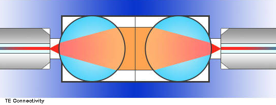 Extreme sensitivity to any contamination on the mating face of an optical interface has been minimized with the adoption of expanded beam technology, which uses lenses integrated in the connector to increase the diameter of the optical beam across the interface. This technology makes a speck of dust have a much smaller impact on the amount of transmitted light.
Fiber optics are now being considered for medium- to relatively short-reach applications in data centers, such as switch-to-switch and switch-to-core, and in some cases, fiber may even make sense inside the box.
Efforts to minimize printed circuit material losses and distortion in high-performance applications have spurred interest in lifting those channels out of the board. One solution has been to transition high-speed signals to shielded twinaxial cable attached immediately adjacent to an ASIC or SERDES device. Signal attenuation and distortion is much reduced in these cables, which jump over the surface of the PCB and often terminate to an I/O connector mounted on the equipment faceplate.
Another more recent solution is co-packaged optics, which locates the electro-optic conversion process on a common substrate with a SERDES or switch chip and uses optics to bring the signal directly to the I/O panel. The result is less distortion and higher port density.
The technology used to achieve this integration is silicon photonics, which seeks to integrate multiple components of an optical transmitter and/or receiver on a silicon chip. The objective is to replace electrical pulses with photonic signaling. For years, scientists tried unsuccessfully to build a practical laser on silicon. More recently, they have chosen to concentrate on separate laser source and photonic chips mounted on a common substrate. Silicon photonic devices can integrate multiple functions, including, modulators, SERDES, optical amplifiers, detectors, filters, couplers, and splitters with electronic logic, memory, and driver circuits on the same chip.
The advantages this technology offers include:
- Signal density that is measured in micrometers
- Higher speed transmission
- Silicon waveguides can be patterned on a common substrate along with electrical conductors
- Uses existing high-volume IC manufacturing, processes, and wafer test equipment
- Enables the ability to create electronic and optical components on the same microchip
- Enables electro-optic conversion on the same chip
- Reduced power consumption
- Increased integration provides increased system density
- Lower system cost through automation
This technology is still more of a concept than a product today, but several suppliers, including Intel, have demonstrated prototypes that illustrate the performance advantages of co-packaged optics, and many engineers see silicon photonics as a long-term solution to the growing challenges of bandwidth bottleneck as well as I/O panel density.
Like this article? Check out the rest of Bob’s Technology Trends Series, our other high-speed, fiber optic, and networking articles, our Telecom/Datacom and Wire & Cable Assemblies Market Pages, and our 2020 and 2019 Article Archives.

- Agentic and Neuromorphic Computers Enable the Future of Digital Computing - May 26, 2026
- OFC 2026: High-Speed Networking in the AI Era - April 7, 2026
- DesignCon 2026 - March 17, 2026